




Description
The semiconductor industry is expanding rapidly due to advancements in artificial intelligence, IoT devices, automotive electronics, high-performance computing, and advanced data centers. As demand for faster and more efficient chips grows, the need for skilled VLSI and physical design engineers continues to increase worldwide.
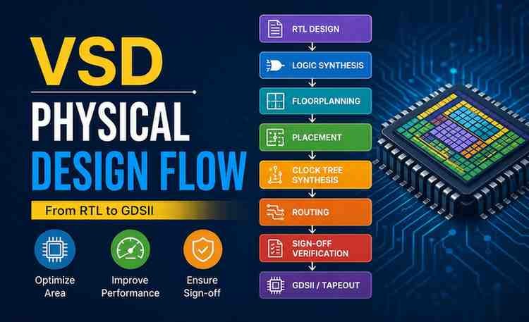
The VSD – Physical Design Flow course is designed to introduce learners to the complete backend VLSI physical design process used in modern semiconductor chip development. The course focuses on practical industrial concepts such as floorplanning, placement, clock tree synthesis, routing, timing analysis, and parasitic extraction.
In this detailed review, we will analyze the course structure, teaching quality, strengths, weaknesses, career value, and whether this course is suitable for aspiring VLSI engineers.
What Is VSD – Physical Design Flow?
The course is a backend VLSI design training program that explains how digital chip designs move from logical representation to physical silicon implementation.
The training covers important stages of physical design including:
- Floorplanning
- Placement optimization
- Clock Tree Synthesis (CTS)
- Static Timing Analysis (STA)
- Routing
- Design Rule Check (DRC)
- Signal integrity
- Parasitic extraction
- SPEF file concepts
The course uses simplified explanations and visual learning techniques to make difficult semiconductor concepts easier to understand.
Why Physical Design Matters in VLSI
Physical design is one of the most critical stages in semiconductor development because it converts synthesized logic into an actual chip layout that can be manufactured.
The complete flow involves optimizing:
- Power consumption
- Performance
- Area utilization
- Timing closure
- Routing efficiency
- Signal integrity
Modern chip companies working on CPUs, GPUs, AI accelerators, networking chips, and automotive electronics rely heavily on backend VLSI engineers.
This course introduces these industrial concepts in a beginner-friendly manner while explaining how large chips are physically implemented.
Course Structure and Curriculum
The course is divided into multiple sections covering the entire backend physical design workflow.
1. Physical Design Flow Overview
The introductory section explains the overall semiconductor backend process.
Topics include:
- Physical design stages
- Chip implementation flow
- Placement optimization
- Clock distribution basics
- Timing closure
- Routing overview
This section builds foundational understanding before moving into advanced concepts.
2. Floorplanning
Floorplanning is one of the most important stages in chip implementation.
The course explains:
- Utilization factor
- Aspect ratio
- Pre-placed macros
- Decoupling capacitors
- Power planning
- Pin placement
- Placement blockages
The instructor simplifies chip layout organization using practical examples and visual explanations.
3. Placement Optimization
Placement directly impacts chip timing and routing congestion.
The course covers:
- Netlist binding
- Standard cell placement
- Wirelength optimization
- Capacitance estimation
- Delay optimization
These concepts are highly relevant in real semiconductor workflows.
4. Timing Analysis
Timing analysis is often considered one of the most difficult topics for beginners in VLSI.
The course explains:
- Setup timing
- Clock uncertainty
- Clock jitter
- Multiple clock domains
- Data slew checks
- Timing margins
The lessons aim to simplify static timing analysis using conceptual and visual explanations.
5. Clock Tree Synthesis and Signal Integrity
Clock Tree Synthesis (CTS) is essential for distributing clock signals efficiently across a chip.
Topics include:
- Clock tree routing
- Buffer insertion
- H-tree algorithms
- Crosstalk
- Clock shielding
- Real clock timing analysis
These are advanced backend concepts frequently discussed in semiconductor interviews.
6. Routing and Design Rule Check
Routing converts logical connections into physical metal interconnects.
The course introduces:
- Maze routing
- Lee’s algorithm
- Routing constraints
- Design Rule Check (DRC)
This section helps learners understand how physical interconnections are implemented inside semiconductor chips.
7. Parasitic Extraction
Parasitic extraction is important for timing signoff and performance analysis.
The course discusses:
- SPEF format
- Resistance and capacitance extraction
- RC modeling
- Post-routing analysis
These concepts are essential for understanding modern physical verification workflows.
Teaching Style and Learning Experience
One of the unique aspects of this course is its infographic-based micro-learning format.
The teaching style focuses on:
- Short conceptual videos
- Simplified visual explanations
- Industrial terminology
- Practical semiconductor workflows
- High-level conceptual understanding
The instructor attempts to make difficult semiconductor concepts accessible for beginners entering the VLSI domain.
The overall learning experience is beginner-friendly and focuses heavily on conceptual clarity rather than overwhelming students with advanced mathematics or tool commands immediately.
What Makes This Course Valuable?
Strong Introduction to Backend VLSI
This course provides a simplified introduction to physical design flow for beginners.
It helps learners understand:
- How chips are physically implemented
- How backend workflows operate
- How timing closure works
- How placement and routing affect chip performance
Industry-Relevant Concepts
The course focuses on real semiconductor design stages used in the industry.
This includes:
- Floorplanning
- CTS
- STA
- Routing
- DRC
- Signal integrity
These topics are frequently discussed during VLSI interviews and backend engineering roles.
Beginner-Friendly Explanations
Many VLSI resources become highly mathematical and tool-heavy very quickly.
This course instead prioritizes conceptual understanding first, making it ideal for students and beginners entering the semiconductor field.
Affordable Learning Option
Compared to expensive semiconductor institutes and professional VLSI training programs, this course provides accessible learning at a lower cost.
Pros of the Course
Excellent Conceptual Foundation
The course explains difficult backend VLSI topics in a simplified and understandable way.
Covers Complete Physical Design Flow
Learners gain exposure to the entire backend semiconductor implementation process.
Useful for Interview Preparation
The concepts align with many VLSI backend interview discussions.
Beginner-Friendly Structure
The course is approachable even for learners with limited semiconductor knowledge.
Strong Industry Relevance
Physical design engineers remain highly valuable due to the global semiconductor expansion.
Potential Drawbacks
Limited Hands-On Tool Practice
The course focuses more on conceptual understanding than deep practical EDA tool implementation.
Students seeking advanced practical exposure may need additional experience with:
- OpenROAD
- OpenLane
- Cadence Innovus
- Synopsys ICC2
Some Sections Feel Introductory
Experienced VLSI engineers may find certain portions too high-level or simplified.
Less Focus on Advanced Projects
The course primarily focuses on theory and workflow understanding rather than large industrial projects.
Who Should Take This Course?
This course is ideal for:
- Electronics engineering students
- VLSI beginners
- Semiconductor career aspirants
- ASIC backend learners
- RTL-to-GDS beginners
- Engineering students preparing for VLSI interviews
It is especially useful for learners who want conceptual understanding before transitioning into advanced industrial EDA tools.
Career Opportunities After Learning Physical Design
Understanding physical design can help learners pursue careers such as:
- Physical Design Engineer
- Backend VLSI Engineer
- ASIC Design Engineer
- Timing Analysis Engineer
- STA Engineer
- CAD Engineer
- Semiconductor Verification Engineer
The semiconductor industry continues to grow rapidly due to AI, automotive electronics, edge computing, and advanced chip manufacturing technologies.
Is This Course Enough for a Job?
The course provides a strong conceptual starting point, but backend VLSI jobs usually require additional practical experience.
To become job-ready, learners should also practice:
- Open-source RTL-to-GDS flows
- Timing analysis exercises
- Linux commands
- Tcl scripting
- Verilog basics
- Physical design projects
Combining this course with hands-on implementation tools can significantly improve employability.
Tips to Get Maximum Value from the Course
To improve learning outcomes:
- Study digital electronics fundamentals first
- Learn basic Verilog and RTL design
- Take notes during timing analysis sections
- Practice using open-source physical design tools
- Revise STA concepts multiple times
- Build small RTL-to-GDS projects
- Explore OpenLane and OpenROAD workflows
Consistent practice is essential because VLSI concepts are highly technical.
Summary
The VSD – Physical Design Flow course is a strong introductory training program for learners interested in backend VLSI and semiconductor chip design.





Reviews
There are no reviews yet.